Our research focuses on controlling thin-film growth and interfaces in oxides and 2D materials using Atomic Layer Deposition (ALD). We emphasize defect engineering and structure–property relationships to enable electronic, optical, and energy applications.
Research Focus
- Thin-film growth and interfaces
- Surface chemistry
- Structure–property relationships
- 2D and low-dimensional materials
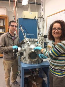
Experimental Approach
- Atomic Layer Deposition (ALD)
- Physical vapor deposition (PVD)
- Integrated thin-film characterization
Our work combines synthesis with detailed characterization to understand how microscopic structure influences measurable material properties.
Why It Matters
Controlling materials at the nanoscale is essential for next-generation electronics, energy systems, and photonic devices. Our work links atomic-scale growth processes to measurable electronic and optical performance.
Capabilities
- Atomic Layer Deposition (ALD)
- Thin-film characterization (ellipsometry, FTIR, electrical transport)
- Access to AFM and SEM facilities
Representative Materials
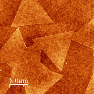
Monolayer MoS2 flakes.

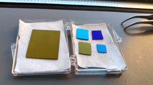
TiO2 thin films with tunable optical response.