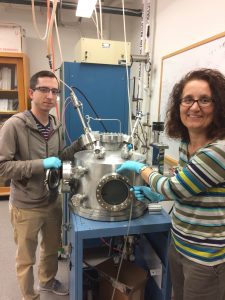
Our research interests are in the deposition and electronic and photonic properties of thin films and their interfaces with semiconductor materials. In addition to conventional semiconductors such as Si and III-Vs (GaAs, InAs) we also study novel materials such as transition metal dichalcogenides (MoS2). We use both chemical (Atomic Layer Deposition) and physical vapor deposition methods to produce thin films on a variety of substrates.
We characterize thin film and interfaces with the goal of understanding:
Film formation mechanisms
Surface Chemistry
Interface properties
Relationship between microscopic structure and film electronic and photonic properties
Additionally, we have used ALD to decorate quantum dots and to fabricate nanostructures.
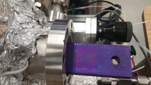
Thin-film characterization techniques available in our lab include Fourier transform infrared spectroscopy, spectroscopic ellipsometry, electrical (CV and IV) measurements, stylus profilometry. Additional facilities housed in the Physics department include Atomic Force Microscopy and Scanning Electron Microscopy. More details can be found under facilities.
Images: Monolayer MoS2 flakes.

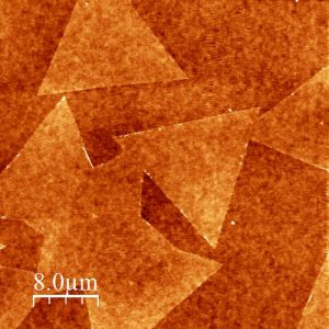
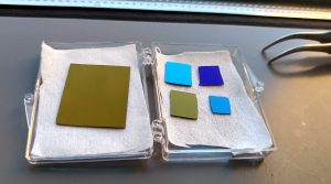
Image: TiO2 films with a different optical response due to variations in their composition